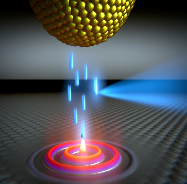
Filming the thermal death of electrons in matter
29.07.2021
 |
|
Image: Scixel. |
- Researchers led by Prof. Otero at IMDEA Nanoscience / UAM have proposed a new method to explore the thermalisation of hot carriers with a time resolution of billionths of a second.
- The work has been published in the prestigious journal Nanoletters.
Madrid, July 29th, 2021. It is well known that a flow of electrons passing through a material, that is, an electric current, increases the temperature of this material due to the so-called Joule effect. This effect, which is used daily in domestic and industrial heaters, hair dryers, thermal fuses, etc., occurs because the new electrons injected into the material cannot go to the lower energy states, because they are already occupied by the electrons of the material and, therefore, they must start their journey with relatively high energies, so they are called hot carriers. However, as they move through the material, hot carriers lose energy through collisions with other electrons and atoms in the solid. The process by which this lost energy is translated into thermal energy and, therefore, into an increase in temperature, is known as thermalisation of hot carriers.
It should be noted however that this well-known effect takes place for very high electron fluxes, which can reach billions of electrons per second in electronic devices in use. Therefore, it gives us information about the collective behaviour of a myriad electrons, but how long it takes each of them to lose their energy is a generally difficult question to answer experimentally.
How long it takes each of the electrons to lose their energy is a generally difficult question to answer experimentally.
In an article that has recently been published in the prestigious journal Nano Letters, a group of Spanish researchers has proposed a new method to explore the thermalization of hot carriers with temporary resolution of billionths of a second. The work, which results from a collaboration between the Autonomous University of Madrid, IFIMAC, the Madrid Institute for Advanced Studies in Nanoscience (IMDEA Nanociencia), the Donostia International Physics Center (DIPC) and the University of the Basque Country/Euskal Herriko Unibertsitatea, has used a Scanning Tunnel Microscope to inject electrons into a silver surface at a rate thousand times lower than that corresponding to operating currents in standard devices and has examined the energy distribution of the emitted light at the junction in response to electron injection.
A naïve view of the law of Conservation of Energy would imply that photons should not be emitted with energies greater than the voltage applied to the junction: the experiment, on the contrary, shows that, although the number of photons with energies greater than the applied voltage is very small, it is not completely zero. In its work, the consortium led by Prof. Roberto Otero explains this phenomenon as the result of taking into account the temperature of the electron cloud of the solid, and allows to extract this temperature from the energy distribution of the photons with energies above the voltage.
This analysis shows that the temperature of the electron cloud and that of the material itself do coincide for high temperatures and low currents. However, as the current is increased, the estimated electronic temperature increases above the sample temperature. The authors rationalize this behaviour taking into account that, by increasing the current, the average time between the injection of consecutive electrons decreases. When this time is less than the time corresponding to the thermalisation of hot carriers, the second electron injected notices the electron cloud temperature is higher than the one of the sample, because the energy of the first electron has not yet been completely dissipated. If the injection of the second electron results in the emission of light, the energy distribution of the light with energies above the voltage will reflect the temperature of the electron cloud at the time of injection. In this way, by measuring the emission of light with energies above the voltage at different currents it is possible to follow the speed with which the thermalisation process takes place.
The study offers a new way of measuring the electronic temperature of solids with atomic spatial resolution.
The importance of these results is based on three fundamental pillars: First, it clarifies the nature of photon emission above the applied voltage and shows how this fact is perfectly consistent with current scientific knowledge; second, it offers a new way of measuring the electronic temperature of solids that, by using a scanning tunnel microscope, would allow the study with atomic spatial resolution; finally, it offers a new tool to study the thermalisation processes of hot carriers one at a time. For all these reasons, the authors are confident that this work is essential for the design and characterization of nanoscale thermal and luminescent devices, and could have important implications for the design of nanometer catalysts for different chemical reactions, or the manufacture of nanometer lasers that could work with extraordinary low pump powers.
This work is a collaboration between research groups at Madrid’s Institute for Advanced Studies in Nanoscience (IMDEA Nanociencia), the Condensed Matter Physics Center (IFIMAC) at the Autonomous University of Madrid, the Donostia International Physics Center and the University of the Basque Country/EHU, and has been co-financed by the "Severo Ochoa Centre of Excellence" award, awarded to IMDEA Nanoscience in 2017.
Reference:
Alberto Martín-Jiménez, Koen Lauwaet, Óscar Jover, et al. Electronic Temperature and Two-Electron Processes in Overbias Plasmonic Emission from Tunnel Junctions. Nano Lett. 2021.
DOI: 10.1021/acs.nanolett.1c00951
Contact
Prof. Roberto Otero
roberto.otero [at]imdea.org
Twitter: @rotero_lab
IMDEA Nanociencia Outreach Office
divulgacion.nanociencia [at]imdea.org
Twitter: @imdea_nano
Facebook: @imdeananociencia
Instagram: @imdeananociencia
Source: IMDEA Nanociencia


