Beyond van der Waals: next generation of covalent 2D-2D heterostructures
25.04.2022
 |
|
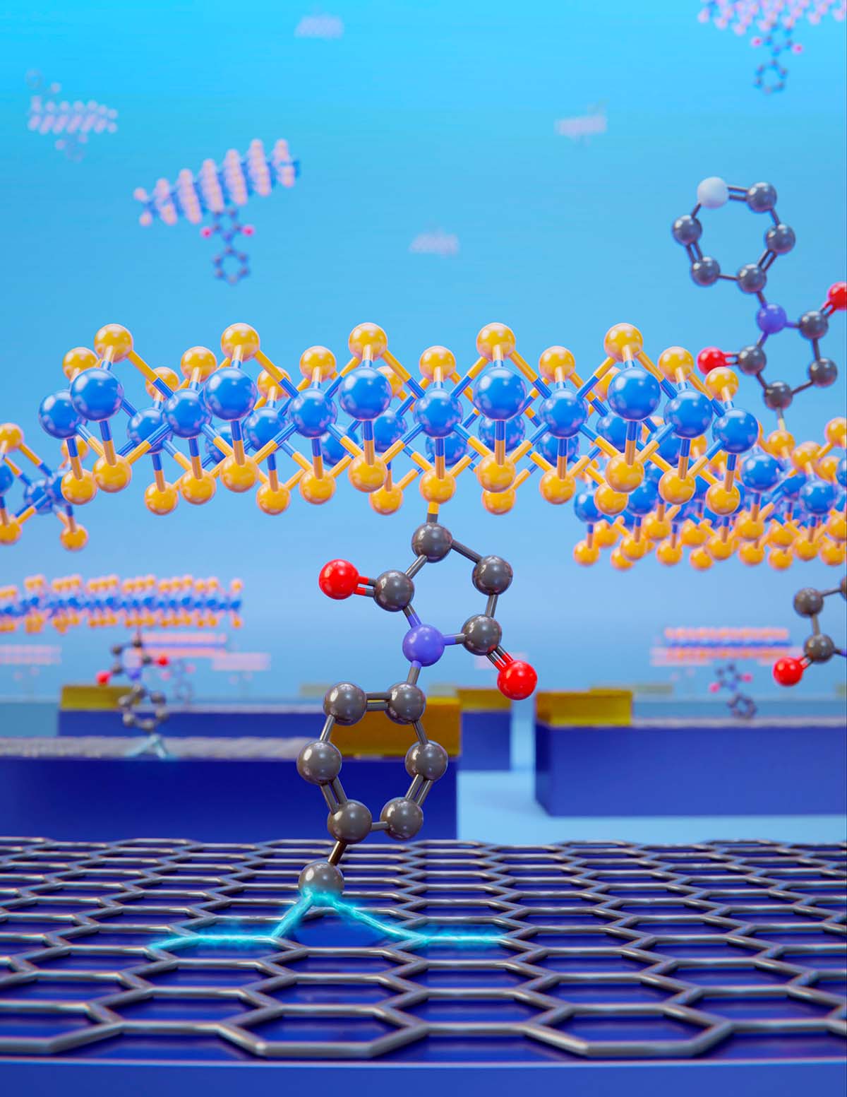
2D structures of MoS2 are connected to graphene using a covalent bond. Credit: Patricia Bondía. |
- A team of scientists at IMDEA Nanociencia have velcroed 2D structures of MoS2 and graphene using a covalent connection for the first time
- The 2D-2D structures were used to build robust field effect transistors with controlled electronic communication, interface chemical nature and interlayer distance.
- The electronic properties of the system are dominated by the interface of the two covalently bonded layered materials.
Madrid, April 25th, 2022. The most widespread method for the synthesis of 2D-2D heterostructures is the direct growth of materials on top of each other. 2D structures are atomically thin layered materials that can be stacked to build functional heterostructures. In such structures built by atomic deposition, 2D layers are weakly bonded by van der Waals interactions and can be taken apart in some solvents or thermal processes. The lack of control over the interface of the two materials in terms of electronic communication, chemical nature or interlayer distance thus impedes the construction of robust multi-purpose devices.
A team of researchers led by Enrique Burzurí and Emilio M. Pérez at IMDEA Nanociencia (Madrid, Spain) have connected covalently for the first time layers of 2D materials: MoS2 and graphene. The team has used the tools of synthetic chemistry to sew several flakes of MoS2 to single-layer graphene devices, using a bifunctional molecule with two anchor points. The results, published now on Nature Chemistry, show that the final electronic properties of the heterostructure are dominated by the molecular interface.
Researchers have connected covalently for the first time layers of 2D materials
The combination of the semiconducting properties of transition metal dichalcogenide MoS2 with the high carrier mobility of graphene is particularly attractive for applications. The group built field-effect transistors (FET) to test the electrical properties of the structure. They found a modification in the gate-voltage characteristic, with a shift of the Dirac cone towards positive voltages and a reduction of the current at the minimum. This current suppression in graphene is unambiguously associated to the disruption of the sp2 hybridization into sp3 due to the formation of covalent bonds. A control experiment with pristine MoS2 suspended on top of graphene showed no significant changes in the D band intensity. Interestingly, the charge carrier mobility is conserved after functionalization and covalent bond formation between MoS2 and graphene, being the degree of graphene doping controllable via the degree of functionalization.
The fabrication of these 2D-2D covalent heterostructures is relatively easy. A silicon substrate containing a single-layer graphene sheet was immersed in a suspension of functionalized MoS2 in water at 35 °C. Two hours of functionalization were enough to promote the covalent bonding in most of the graphene spots. To confirm the covalent functionalization, Raman spectroscopy was performed to track the transformation of sp2 carbon atoms of the graphene to sp3 as indication of formation of a new C-C bond.
Interview to the authors
How would you explain your work to someone who has no knowledge of the field?
Enrique Burzurí (EB): 2D materials are extremely (atomically) thin materials that present interesting properties for electronic applications. Depending on the nature of the material, these properties can be different (good electrical conductivity, sensitivity to light, etc). This is why scientists are trying to combine two or more of these materials into a new one. The most widespread method to do this is by manually stacking one material on top of the other one piece at a time. Instead, we use chemistry to bond the materials into strong structures where a small molecule is used as linker and as modulator of the electrical properties of the final material.
Emilio M. Pérez (EMP): Exactly! When trying to combine the best of two materials, most scientists have focused on simply piling them up together. What we do here is to actually design a molecular “Velcro” that is reactive towards one material on one end, and towards the other on the other end, so that we can put them together, easier, faster, many flakes at a time…Also, and this is important, the molecular linker actually affects the properties of the final assembly, so we add one more degree of control to the heterostructure.
Why should an average person care about this research? What are some potential real-life applications?
EB: The approach we have followed has the potential to reduce costs and achieve a better control in the fabrication of new electronic devices based on 2D materials. These breakthroughs would bring the long-time sought implementation of 2D materials in real-life electronics closer.
EMP: This piece of work is best viewed as the development of a tool. We are providing a new means to make devices based on 2D-2D heterostructures. Besides possibly reducing costs of fabrication, as Enrique points out, this has potential implications in what the devices can do (for instance, enabling a new function), and on how well they do it (for example, improved performance of a sensor).
Why did you choose to research this topic?
EMP: The chemistry of 2D materials is in itself very interesting, because it is very challenging. All atoms look the same, and are typically not very reactive, so it is difficult to do chemistry on them, and difficult means fun! Also, the privilege of chemistry is that we can transform matter, so that we can make it useful (or just more interesting). In this case, for instance, by sticking together two 2D materials easier and with better control.
EB: For me, the combination of 2D materials into heterostructures is one of the most active fields in materials science. I find very interesting that this research field may lead not only to new technologies but also to new exciting physical phenomena.
What is the most exciting thing about your results?
EB: I find very exciting that thanks to this chemical approach we can fabricate hundreds of these electronic devices in a single step. Moreover, this technique can be extended to other more exotic materials so we can create a new generation of electronic devices with properties that can complement electronics
EMP: I believe the simplicity of the method is what’s most exciting. Everything is done under mild conditions, at or close to room temperature, using common laboratory equipment and reagents… This also makes it very robust and reproducible: we’ve made literally hundreds of devices and the method just works!
What is the novelty, the innovation beyond the state of the art of these results?
EMP: It’s always difficult to quantify these things…especially when it is your own research you are talking about. Perhaps the easiest way to gauge the novelty is that so far, the stacking of 2D materials on top of one another relied exclusively on van der Waals forces to the point that the whole field is often called “van der Waals heterostructures”. Van der Waals forces are great, you know? as a supramolecular chemist, I love noncovalent forces, but if you think of it, it is rather limiting to just have the one option…particularly considering that the properties of the final heterostructure depend crucially on how the nanomaterials are interfaced (I recently heard Prof. Luis Hueso state that “the interface is the device”). On the other hand synthetic chemistry is the paradigm of atomic-scale control. With this piece of work, we bring the huge toolbox of chemistry to the game of making 2D-2D heterostructures… I believe it is fair to say it is a noteworthy contribution.
EB: We have changed the way 2D heterostructures are made. For the first time we have used chemistry to covalently bond 2D materials and in-situ form several electronic devices at the same time.
For the first time, researchers have used the tools of chemistry to covalently bond 2D materials. The results show the power of the chemical approach to build MoS2-graphene heterostructures beyond van der Waals preserving the carrier mobility of graphene for high performance FET devices. The vertical covalent connection brings an additional lever to the final properties of nanodevices beyond the intrinsic properties of the materials, and has the potential for facile high-throughput homologation.
This work is a collaboration among researchers at IMDEA Nanociencia, Universidad Autónoma de Madrid, CEITEC Masaryk University Kamenice, Universidad de Zaragoza, INMA and CIBER-BNN, and has been cofunded by the European Research Council (ERC) trough StG MINT and PoC PINT grants and MSCA PD grant 892667 TweeTERS.
Reference:
M. Vázquez Sulleiro et al. A chemical approach to 2D-2D heterostructures beyond van der Waals: high-thorughput on-device covalent connection of MoS2 and graphene. Nat. Chemistry. 2022.
DOI: 10.1038/s41557-022-00924-1

Contact
Dr. Enrique Burzurí
enrique.burzuri [at]uam.es
https://nanociencia.imdea.org/functional-nanoscale-materials-and-devices/home
Twitter: @enburz
Prof. Emilio M. Pérez
emilio.perez [at]imdea.org
https://nanociencia.imdea.org/chemistry-of-low-dimensional-materials/home
Twitter: @emiliomperezlab
IMDEA Nanociencia Dissemination and Communication Office
divulgacion.nanociencia [at]imdea.org
Twitter: @imdea_nano
Facebook: @imdeananociencia
Instagram: @imdeananociencia
Source: IMDEA Nanociencia


