Engineering the phase and properties of 2-dimensional MoTe2
27.07.2022
 |
|
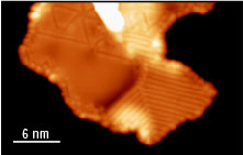
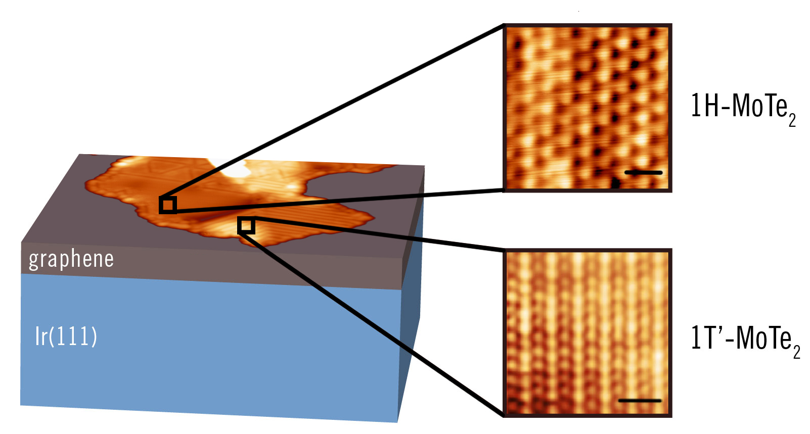
MoTe2 island on graphene with different 1T’/1H phases interfaces. The scalebar size is 6 nanometres. Credit: Nanoscale. |
-
The work by the IMDEA Nanociencia group of Dr. Manuela Garnica reports on the synthesis and characterization of different phases in single-layer MoTe2 on graphene.
- The same material exhibits different electronic properties depending on the location.
- The great control achieved over the fabrication of 2D MoTe2 structures opens new perspectives in the future phase-engineering electronics.
Madrid, July 27th, 2022. The application of 2-dimensional materials in optoelectronic devices is sometimes hampered by the electrical barrier between the electrodes and the materials itself. This is called a Schottky contact: a potential energy barrier for electrons formed at a metal–semiconductor junction, which represents an important throwback when building efficient devices. A possible solution to reduce the contact resistance is to build a continuous a lateral structure with different properties: semiconducting and metallic phases of the same material.
In the field of electronics, transition metal dichalcogenides are interesting materials that show a wide range of physical properties from semimetallic to semiconductors, superconductors or insulators, that make them ideal candidates for applications. Molybdenum ditelluride (MoTe2) is an excellent material for the purpose because, contrary to other tellurides, exhibits two stable phases at ambient temperature.
Most of the results regarding phase engineering in 2D transition metal dichalcogenides have been obtained for exfoliated flakes. However, while the quality of these layers is suitable for fundamental research, the thickness inhomogeneities, high defect density and uneven interfaces are still jeopardizing real applications. Epitaxial growth - depositing a thin layer of single material following the crystal structure of a substrate- of 2D materials is a scalable process to large-area production with a good control of thickness and structural quality of the layers.
The recent work by the IMDEA Nanociencia group of Dr. Manuela Garnica reports on the synthesis and in situ characterization of different phases in single-layer MoTe2 on graphene. Tuning the growth parameters, such as Telluride/Molybdenum ratio and sample temperature, the team was able to achieve phase engineering in this material to produce large areas of pure semimetallic phase. In their scanning tunnelling microscope images, they could clearly identify two phases: the semiconducting hexagonal phase (1H), and the semimetallic distorted octahedral phase (1T′) in large islands of tens of nanometers in size.

The MoTe2 layers remained decoupled from the substrate due to the weak interaction with the intermediate layer of graphene. This is important for keeping the properties of MoTe2 intact. In addition, graphene exhibits ultra-high mobility and gate tuneable conductivities. It has been demonstrated that by combining graphene with transition metal dichalcogenides one can improve their properties such as mobility, which opens up new opportunities for switching and transport.
The idea is simple: the same material exhibits different electronic properties depending on the location. This consists a great opportunity for fabricating electronic devices. The junction of a semiconducting phase as channels and a metallic phase of the same material as electrodes produces an ohmic contact with low resistance and eases current conduction from metal to semiconductor and vice versa.
The study, which has been published in Nanoscale, develops a direct synthetic route to produce large areas of a pure semimetallic phase of 2-dimensional MoTe2 as well as lateral heterostructures, combining this semimetallic phase with a semiconductor one. The study also characterized them for first time at atomic scale. The great control achieved over the fabrication of 2D MoTe2 structures with different electronic properties in a decoupling layer opens new perspectives to combine semiconductor and a semimetal stable homostructures at room temperature in the future phase-engineering electronics.
“The control and characterization at atomic scale of the interface between semiconducting-semimetallic MoTe2 phases constitutes a valuable source of knowledge for potential technological applications”, Dr. Garnica says. “Phase engineering creates then new horizons in the design of materials with specific properties. Scanning tunnelling microscope (STM) offers the possibility of investigating these heterostructures with unprecedented resolution.”
This research result is a collaboration between researchers at IMDEA Nanociencia and Universidad Autónoma de Madrid, and is cofunded through the Postdoctoral Junior Leader Fellowship Programme from “la Caixa” to Manuela Garnica; and through the Severo Ochoa Centre of Excellence award to IMDEA Nanociencia.
Reference:
Joan Ripoll-Sau, Fabian Calleja,Pablo Casado Aguilar, Iván M. Ibarburu, Amadeo L. Vázquez de Parga, Rodolfo Miranda and Manuela Garnica. Phase control and lateral heterostructures of MoTe2epitaxially grown on graphene/Ir(111). Nanoscale. 2022.
DOI: 10.1039/D2NR03074H
The post-print is available* from the IMDEA Nanociencia Repository: https://repositorio.imdeananociencia.org/handle/20.500.12614/3140
Contact
Dr. Manuela Garnica
manuela.garnica [at]imdea.org
https://nanociencia.imdea.org/nanoscale-imaging-of-2d-materials/group-home
Twitter: @ManuelaGarnicaA
IMDEA Nanociencia Dissemination and Communication Office
divulgacion.nanociencia [at]imdea.org
Twitter: @imdea_nano
Facebook: @imdeananociencia
Instagram: @imdeananociencia
Source: IMDEA Nanociencia


