Researchers analyze the picoantenna-like directional behaviour of tunnel junctions formed by surface defects at the atomic scale
05.11.2024
 |
|
Electromagnetic field inside the STM cavity on a terrace of atoms. Credit: Patricia Bondía. |
- The profile of the light collected in a STM experiment changes when the tip is placed on an atomic step.
- This phenomenon can be exploited to build picoantennas, nanoscale elements that direct light.
| Tweet |
Madrid, 5th November, 2024. Researchers from Madrid explain a phenomenon that allows the direction of light emission to be controlled at the atomic scale. The paper provides a detailed explanation of how a single atom can change the directional profile of the light emitted in experiments with scanning tunnelling microscopes (STMs).
IMDEA Nanociencia's 'Photon STM' laboratory is one of the four tunneling microscopes that this institute, located on the campus of the Autonomous University of Madrid, has. The peculiarity of this instrument? This STM microscope can measure the optical properties of samples since it is equipped with an extension that allows researchers to collect the light emitted during the experiments.
The manipulation of light at the nanometer scale, below its wavelength, is interesting because the properties of light that are picked up in the far field are determined by what happens in the near field. This manipulation can be carried out in STM microscopes because the electromagnetic field is extremely confined between two metal nanostructures, the tip of the microscope and the sample, separated by a typical distance of 1 nanometer. This configuration is called a nanocavity. If an element is introduced into this nanocavity, such as an atomic defect, the system is called a picocavity and has unique properties. It has been observed that, by introducing atomic steps into the nanocavities, it is possible to modify the direction of light emission in the experiments. This phenomenon, which researchers had previously observed, lacked a scientific explanation until now.
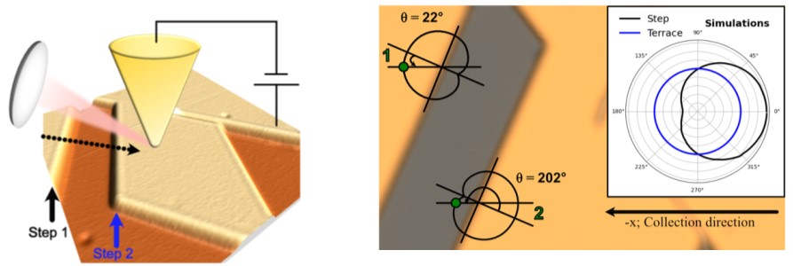
The 'Photon STM' research group at IMDEA Nanociencia, led by Alberto Martín Jiménez and Roberto Otero, has made measurements of the radiated light in an experiment with a picoantenna composed of a gold STM tip and a smooth surface of silver atoms with an atomic step. During a typical measurement with an STM microscope, the tip travels across the sample, sweeping the surface back and forth as it picks up the signal. The researchers observed that the light emitted by each electron tunneling with the right energy on a monatomic step can be greater or less than that collected when the electron is injected into the atomically flat part of the surface.
By a comprehensive characterization of the light emitted by many steps, the researchers discovered that the parameter that governs the intensity of light per electron is the relative orientation between the directions of the step and the direction of light collection, thus demonstrating that the emission of light is not equally distributed in all directions of space, but some are preferred to others with a cardioid-type directional profile.

In collaboration with Antonio Fernández, researcher at IFIMAC-UAM, the authors elucidated the mechanism by which light emission is modified. In their work, recently published in Science Advances, they explain that in cavities as small as those between the tip and the STM sample, an atomic size defect is enough to cause a significant redistribution of the electric field, which becomes very different on both sides of the step, thus explaining why the angular profile of light emission depends on the orientation of the step. This phenomenon can be exploited to make a picoantenna, an element at the nanoscale with which to control the directionality of the emitted light.
In summary, in order to determine the electromagnetic field (light) emitted in the near field, it is not only necessary to take into account the point-sample structure of the microscope, but also the configuration and defects of the sample being swept, at the atomic scale, since a single atomic defect can modify the direction in which this radiation is emitted.
The authors see potential in this method to eventually tune the direction of light emission from molecules, quantum dots, or other quantum emitters. Investigating the optical properties of atomic objects is crucial not only to advance our knowledge but also to be able to design systems that have application, for example, in quantum computing.
This work has been carried out at the Madrid Institute for Advanced Studies (IMDEA Nanociencia) and the Centre for Condensed Matter Physics (IFIMAC-UAM), and has been co-funded with the Severo Ochoa Excellence accreditation to IMDEA Nanociencia (CEX2020-001039-S), the María de Maeztu Excellence accreditation to IFIMAC (CEX2020-000805-M), the MSCA-PF STED grant (101108851) and the MAD2D regional project of Comunidad de Madrid.
Glossary:
- Nanocavity: (dielectric gap) a gap formed, in the case of this article, between the tip of an STM microscope and the sample, which are about 1 nanometer apart.
- Picoantenna: a term adopted by the authors to designate the system formed by an atomic defect (such as a step of atoms) within a nanocavity.
- Scanning tunnelling microscope (STM): Instrument for taking images of surfaces at the atomic level, based on the concept of tunneling. The tip is placed close to the surface, and electrons can "jump" from the tip to the sample thanks to the quantum tunneling effect, creating a current that can be measured, and that depends on the distance at which the tip is located. If the tip sweeps the surface, a relief map, or image, is created.
Reference:
David Mateos, Óscar Jóver, Miguel Varea, Koen Lauwaet, Daniel Granados, Rodolfo Miranda, Antonio I. Fernández-Domínguez, Alberto Martín-Jiménez, Roberto Otero. Directional picoantenna behavior of tunnel junctions formed by an atomic-scale surface defect. Science Advances 10, eadn2295(2024). DOI: 10.1126/sciadv.adn2295
![]() https://repositorio.imdeananociencia.org/handle/20.500.12614/3811
https://repositorio.imdeananociencia.org/handle/20.500.12614/3811
Contact:
Alberto Martín Jiménez
Photon STM Group
https://nanociencia.imdea.org/photon-stm/home
Oficina de Divulgación y Comunicación en IMDEA Nanociencia
divulgacion.nanociencia [at]imdea.org
Twitter: @imdea_nano
Facebook: @imdeananociencia
Instagram: @imdeananociencia
Source: IMDEA Nanociencia.
IMDEA Nanociencia Institute is a young interdisciplinary research Centre in Madrid (Spain) dedicated to the exploration of nanoscience and the development of applications of nanotechnology in connection with innovative industries.


